SUPERCONDUCTING FILMS
- YBa2Cu3O7-x films of thickness more than 0.5 μm have become a promising materials for high-power electronics and microwave device applications.
- Thickness of several London penetration depth is required in microwave devices to minimise the microwave signal losses.
- Increase of YBCO film thickness allows us to increase the value of critical current.
- Growth of thick films meets significant difficulties like deterioration of film structure quality, change of preferred growth orientation, diffusion of substrate atoms in the film.
Investigation of YBCO film growth
- Investigation of buffer layer growth to get minimum disorientation between substrate and YBCO film, and to minimize diffusion of substrate atoms in the film.
- Initial stages of YBCO film growth (Scanning electron microscopy image, island concentration, phase structure)
- Structure characteristics of thick YBCO films with second phase inclusions and holes (X-ray diffraction, Scanning electron microscopy image, Rutherford backscattering analysis)
- Microwave and direct current characteristics of thick YBCO films (surface resistance and critical current measurements)
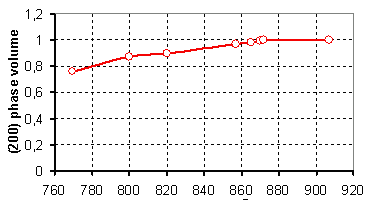
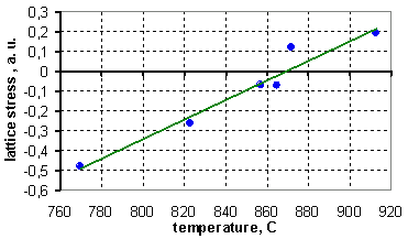
Structure properties of CeO2 buffer layer
CeO2 film is preferentially oriented, with (200) orientation relative to the substrate surface begin from 880°C deposition temperature.
The films obtained at ~870°C exhibit the lowest lattice stress in the absence of any (111)-oriented phase inclusions.
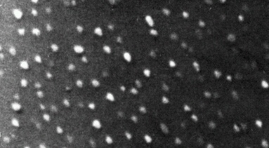
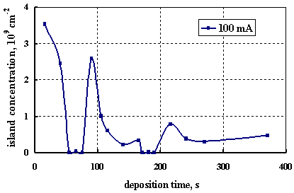
Investigation of initial stages of YBCO film growth
SEM image of island film
Island concentration
The surface morphology of the deposited films was studied by Scanning Electron Microscopy. During the first minutes of growth the concentration of islands varies between less than 107 and 109 cm-2. After ~ 300 s of deposition concentration is about 108 cm-2.
The analysis of the Transmission Electron Microscopy pattern indicates the presence of two phases - YBa2Cu4O8 and CuO. Other phases presented by minor reflections and can not be identified yet.
Structure properties of YBCO films
1.26 micron film diffraction pattern
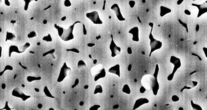
1.26 micron film SEM image
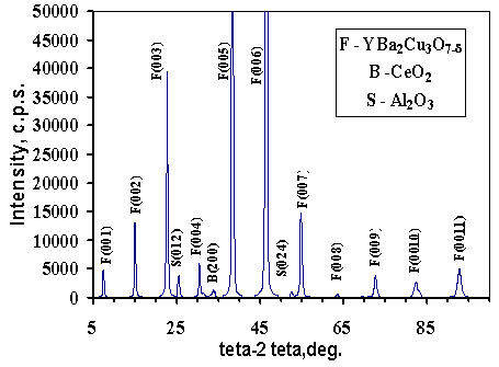
- All permit (00l) peaks are observed by XRD analysis for all films up to thickness 3.6 μm
- a-oriented grains are not observed by XRD analysis for all films of thickness from 0.3 μm to 3.6 μm
- Hole concentration ~ 108 cm-2 remains constant when the thickness increases, while the hole dimensions increases
- Total area of holes, % = 7.8 average size of holes ~ 0.2 μm for 1.26 μm film
Structure properties of YBCO films
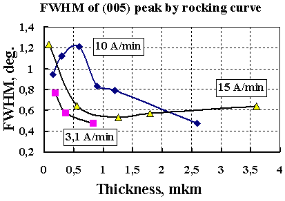
- Full width at half maximum of (005) peak in XRD pattern decreases when the thickness increases, hence the structure of films in terms of grain dimensions and 00l phase orientation improves.
- C-parameter of YBCO lattice increases with thickness up to 11.682 Å for films of thickness ~ 1 μm and more.
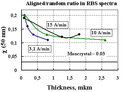
- Aligned/random signal ratio in RBS spectra decrease with thickness confirming the surface layer quality improvement.
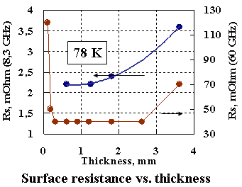
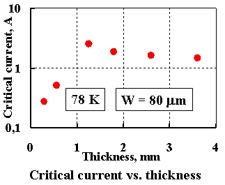
Microwave and direct current characterizations of thick YBCO films
- Up to thickness of about 1 μm average critical current density Jc is independent of the film thickness
- Critical currents of films of thickness ~ 1 μm are three times higher in comparison with films of another thickness
|